
The 2nm Node Has a 16nm Gate and Four Companies Behind It
TechCurrent Staff•Sep 3•10 min read
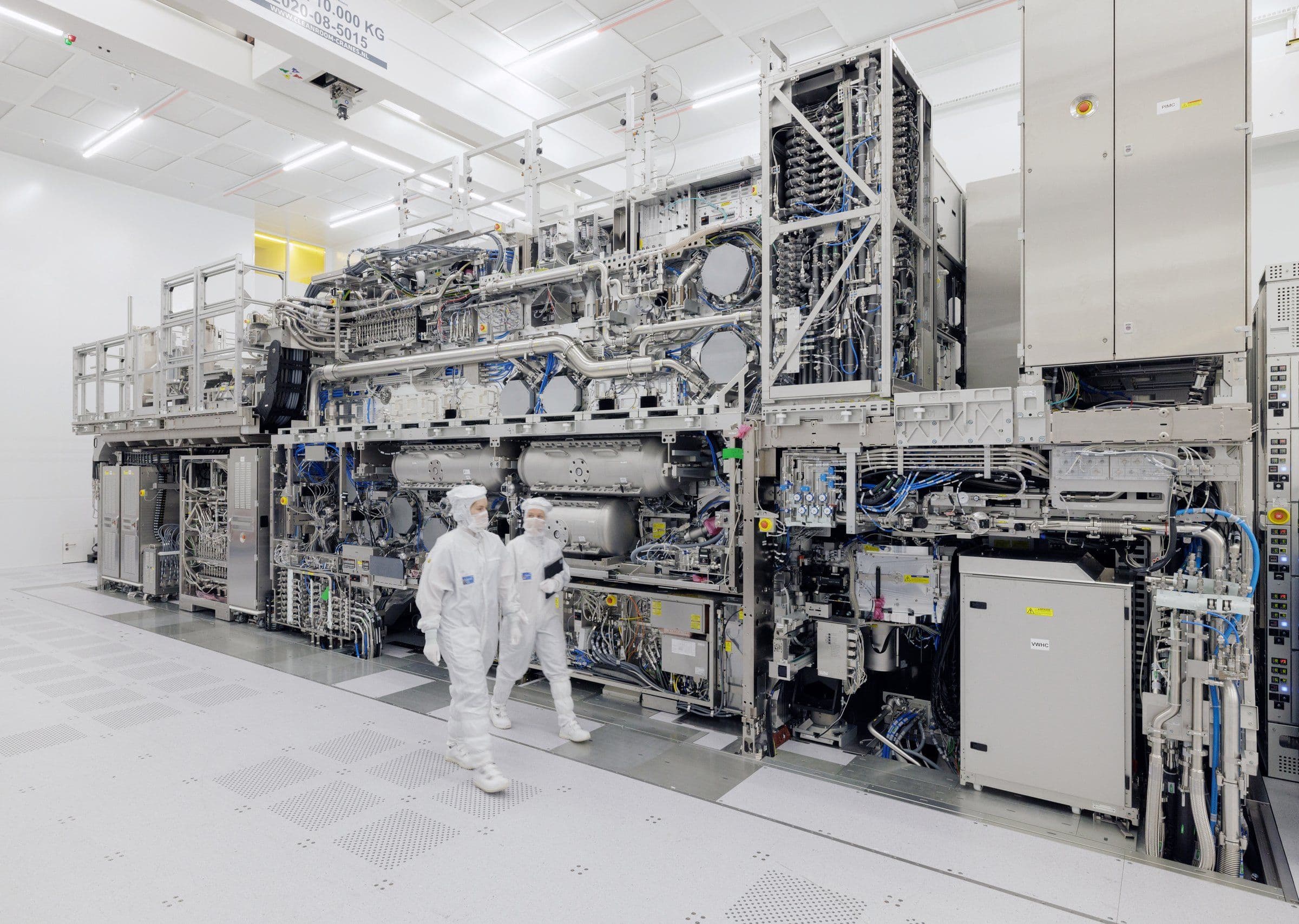
At the node the industry calls 2 nanometres, the transistor gate is 16 nanometres long and the gates repeat every 45 nanometres. Those figures come from imec, in a paper it presented at IEDM in December 2024 describing nanosheet n-FET devices built "for the 2nm node" with, in its own words, "45nm Gate Pitch and 16nm Gate Length" (DOI 10.1109/IEDM50854.2024.10873517). The ASML scanner sold to print 2nm logic in volume, the TWINSCAN NXE:3800E, resolves 13 nm, according to ASML's own product page. No dimension anywhere in the process measures 2 nanometres.
On 25 August Apple announced the M6, which it calls "Apple's first state-of-the-art 2-nanometer chip", shipping in a new Mac mini. Apple named no foundry, and TSMC has not named a customer. What TSMC has confirmed is that N2 entered volume production in 4Q25, and that in the second quarter of 2026 it accounted for 3% of wafer revenue, with CFO Wendell Huang telling investors the third quarter would be supported by "the steep ramp-up of our 2-nanometer technology." That 3% is from the third quarter of volume production on the most advanced process the company has ever run.
Intel's 1.8nm and TSMC's 2nm report near-identical SRAM density
TSMC's public N2 page carries no performance figures, and neither does its A16 page. The numbers live in conference papers and symposium press releases.
The fullest public statement of what N2 delivers is TSMC's own IEDM 2024 paper, by Geoffrey Yeap and colleagues (DOI 10.1109/IEDM50854.2024.10873475). Verbatim: N2 "delivers a full node benefit from previous 3nm node in offering 15% speed gain or 30% power reduction with >1.15x chip density increase", and features the "densest SRAM macro of ~38Mb/mm²".
Intel presented its 18A SRAM work at ISSCC in February 2025 (DOI 10.1109/ISSCC49661.2025.10904657) and reported that "up to 38.1 Mb/mm² is achieved using an HDC SRAM with larger bit array configuration and additional peripheral circuit compaction."
TSMC's densest published N2 SRAM macro is about 38 Mb/mm². Intel's densest published 18A macro reaches 38.1. One is branded 2nm, the other 1.8nm.
Both figures come from the manufacturers' own peer-reviewed papers rather than an analyst's estimate. They are not directly comparable in every respect: SRAM density is one metric among several, and the two macros are different designs. But the node number has stopped tracking geometry. It is shorthand now for a bundle of density, speed and power characteristics a foundry commits to deliver on a schedule. IEEE Spectrum, writing up imec's long-range roadmap in May 2026, put the same thing about a future node bluntly: "It's just a name; there's not necessarily any structure in the transistor that is actually 7 Angstroms."
The fin becomes a stack of sheets
A FinFET, the structure that carried the leading edge from roughly 2011 until now, puts the channel in a vertical silicon fin with the gate wrapped around three of its sides. In a nanosheet or gate-all-around device, the channel is a stack of horizontal silicon sheets and the gate material is deposited entirely around each one. Intel's own definition of its RibbonFET: "the channel is fully surrounded by the gate to enable precise electrostatic control."
The naming is a mess. TSMC says nanosheet, Intel says RibbonFET, Samsung says MBCFET, and imec and Rapidus stick with GAA, all for the same family of device.
The electrostatics matter because at a 16 nm gate length the gate is competing with the drain for control of the channel. Wrapping the channel on four sides instead of three restores that control, which is what allows the supply voltage to keep falling. Most of the "30% power reduction" comes from that rather than from geometry.
A FinFET's drive current comes in integer steps: you want more, you add a whole fin. A nanosheet's effective width is continuously adjustable, because you choose how wide to draw the sheets. Intel's ISSCC paper is explicit that RibbonFET "allows for the flexible adjustment of the effective transistor width to achieve optimal SRAM transistor sizing for power, performance and V_MIN", and reports 0.77x and 0.88x bitcell area scaling for its high-current and high-density cells against comparable FinFET designs. TSMC brands the same freedom NanoFlex.
Backside power delivery is the other half of this generation's change, and it is not arriving on the same schedule at every foundry. Intel shipped it with its first GAA node, pairing RibbonFET with PowerVia in 18A, which it describes as "in high-volume production in the United States" with "up to 18% higher performance at iso power, 38% lower power at iso performance, and 30% chip density improvement" versus Intel 3. TSMC did not. N2 is nanosheet with conventional frontside power; TSMC's backside Super Power Rail arrives with A16, whose risk production the company expects in 2026. Putting 18A's headline numbers next to N2's compares two different bundles of technology.
A14 lands in 2028, A13 in 2029 for 6% of area
TSMC publishes its roadmap once a year at its North America Technology Symposium, and read in sequence the releases are a fairly precise record of what each generation is worth.
| Node | What TSMC says it delivers | Timing |
|---|---|---|
| N2 | 15% speed or 30% power, >1.15x density vs 3nm (IEDM 2024 paper) | volume production 4Q25 |
| N2P | "5% speed enhanced version of N2 with full GDS compatibility" | mass production 2026 |
| N2U | "speed gains of 3-4% or power reduction of 8-10%", plus 1.02-1.03X logic density over N2P | 2028 |
| A16 | nanosheet plus Super Power Rail backside power delivery | risk production expected 2026 |
| A14 | "up to 15% speed improvement at the same power, or up to 30% power reduction at the same speed", "more than 20% increase in logic density" vs N2 | 2028 |
| A13 | "6% area savings from A14" | 2029 |
Sources: TSMC's 2026 symposium release, its 2025 release, and the IEDM 2024 paper.
These are real engineering results, obtained at a cost that has climbed faster than they have.
An EUV scanner averaged €237 million last year
ASML does not publish list prices, but its 2025 annual report discloses net system sales by technology in both units and euros, which amounts to the same thing. Dividing one column by the other gives an audited average selling price per tool.
| Tool class | Units, 2025 | System revenue, 2025 | Average per system (TechCurrent calculation) |
|---|---|---|---|
| High-NA EUV (EXE, 0.55 NA) | 4 | €1,156.9m | €289.2m |
| EUV (NXE, 0.33 NA) | 44 | €10,445.8m | €237.4m |
| ArF immersion | 131 | €10,311.4m | €78.7m |
| KrF | 78 | €1,001.3m | €12.8m |
| i-line | 54 | €307.3m | €5.7m |
Those five classes are an excerpt. ASML's full 2025 system business was 535 units and €24.5bn, including ArF dry scanners and metrology tools not shown here. The same calculation on ASML's 2023 figures gives €172.2m for a 0.33 NA EUV scanner. The average price of the workhorse tool of the leading edge rose 37.9% in two years. One EUV scanner costs about three ArF immersion scanners, or roughly forty of the i-line tools that still pattern mature nodes. In 2025 EUV and High-NA were 48 of the 535 systems ASML shipped, 9% of units, and €11.6bn of €24.5bn in system revenue, 47%.
High-NA is still a drag on the margins of the company selling it: ASML's report says the positive effects on 2025 gross margin were "partially offset by the dilutive impact of EXE systems recognized in sales". CEO Christophe Fouquet reports that by the end of 2025 customers "had run more than 400,000 wafers on High NA EUV systems", and separately credits the NXE:3800E, the 0.33 NA tool doing the actual 2nm printing, with lifting throughput "from 160 wafers per hour to 230 wafers per hour" against the previous system.
TSMC's capital expenditure went from NT$949.8bn in 2023 to NT$1,272.4bn in 2025, a 34% increase, and the company has guided 2026 capex to US$52bn to US$56bn. Its 20-F says what that money is for, verbatim: "installing and expanding capacity, mainly for 2-nanometer and 3-nanometer nodes, including building/facility expansion for Fab 20, Fab 21 and Fab 22." R&D rose 35% over the same two years to NT$246.4bn, an increase the filing attributes to "a higher level of research activities for 10-angstrom, 14-angstrom, and 16-angstrom process technologies". None of those three is in production. TSMC says A16 risk production is expected in 2026, and it has scheduled A14 for 2028.
For scale: 2025 capex alone was roughly a third of 2025 revenue. BCG and SIA estimated in April 2021 that a state-of-the-art fab required "roughly $5 billion (for advanced analog fabs) to $20 billion (for advanced logic and memory fabs) of capital expenditure, including land, building, and equipment", which the report called "significantly higher than, for example, the estimated cost of a next-generation aircraft carrier ($13 billion)". That was five years and two nodes ago; treat it as a floor.
No per-node wafer price exists in public. TSMC does not publish one. Neither does Samsung, Intel or Rapidus. The figures that circulate for N2 and A16 wafers trace back to unnamed supply-chain sources, and the trade press that carries them says so in its own headlines, with words like "reportedly" and "rumors allege". They are not used here.
One number can be computed from the audited disclosures: TSMC's blended revenue per wafer shipped. The 20-F discloses both wafer revenue and 12-inch-equivalent wafer shipments:
| Year | Wafer revenue per wafer shipped |
|---|---|
| 2023 | NT$156,850 |
| 2024 | NT$194,768 |
| 2025 | NT$217,851 (about US$7,000 at the NT$31.11/US$1 rate TSMC states) |
Up 38.9% in two years. This is a TechCurrent calculation from TSMC's audited disclosures, not a TSMC-published figure, and it is a blend across everything the company makes from 0.25 micron to 2 nanometre. It moves with product mix as much as with price, and it is not the price of a wafer. Mix is doing most of the work here: the leading edge is a larger share of what the company ships each year.
N2 runs in two fabs, both in Taiwan
Four organisations worldwide have a 2nm-class gate-all-around process in or approaching production, on their own published statements. TSMC has N2 in volume production since 4Q25. Intel says 18A is in high-volume manufacturing in the United States, though its process overview page also lists the node as "available exclusively as a Design Services Node". Samsung's foundry page says SF2, its "second-generation MBCFET (GAA) technology", "started mass production in 2025", and its 2Q26 earnings deck reports design wins "including 2nm HPC engagements" and guides to a "2nm Gen 2 mobile ramp-up" in the second half of this year, without naming a customer or breaking out foundry revenue at all. Rapidus reported the first successful operation of 2nm GAA transistors on 18 July 2025 and schedules mass production for 2027, so it is not yet in commercial production.
BCG and SIA counted three firms capable of logic at 10nm and below in 2021, and five years and a full architectural transition later the number has not meaningfully grown.
TSMC's 20-F lists N2 volume production in exactly two fabs: Fab 20 in Hsinchu Science Park and Fab 22 in the Southern Taiwan Science Park. As of the end of 2025 the most advanced volume node at Fab 21 in Arizona was 5nm.
The customer list is concentrating too. TSMC's ten largest customers accounted for 70% of net revenue in 2023, 76% in 2024 and 78% in 2025. Its largest single customer is 19% of revenue and its second is 17%, the latter having risen from 11% in two years. When a full node buys 15% and the tool that prints it averages €237m, a leading-edge tape-out only pays for products that ship in enormous volume or sell at enormous margin, which on TechCurrent's reading leaves phones and AI accelerators and not much else. Fewer designs clear that bar each generation.
Related from TechCurrent: [Hardware](https://techcurrent.tech/category/hardware), our running coverage of silicon and the supply chains behind it.
Apple has confirmed 9 September and nothing about the chip
Apple's events page lists 9 September at 10 a.m. Pacific and nothing about the contents. Qualcomm has confirmed that Snapdragon Summit runs 22 to 24 September under the theme "Unleash the Extraordinary", and has published nothing about the process node of anything it will show there. MediaTek has published nothing in 2026 about a 2nm part at all. The widespread expectation that both companies launch 2nm silicon in late September rests on the calendar and on industry inference, not on any statement either has made.
What is on the record is the M6, a 2nm chip in a Mac mini since 25 August, and 3% of TSMC's wafer revenue in the quarter before the ramp began in earnest.
“TSMC's densest published N2 SRAM macro is about 38 Mb/mm². Intel's densest published 18A macro reaches 38.1. One is branded 2nm, the other 1.8nm.”
Reporting by TechCurrent Staff · TechCurrent